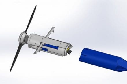
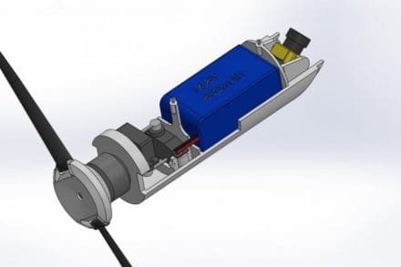
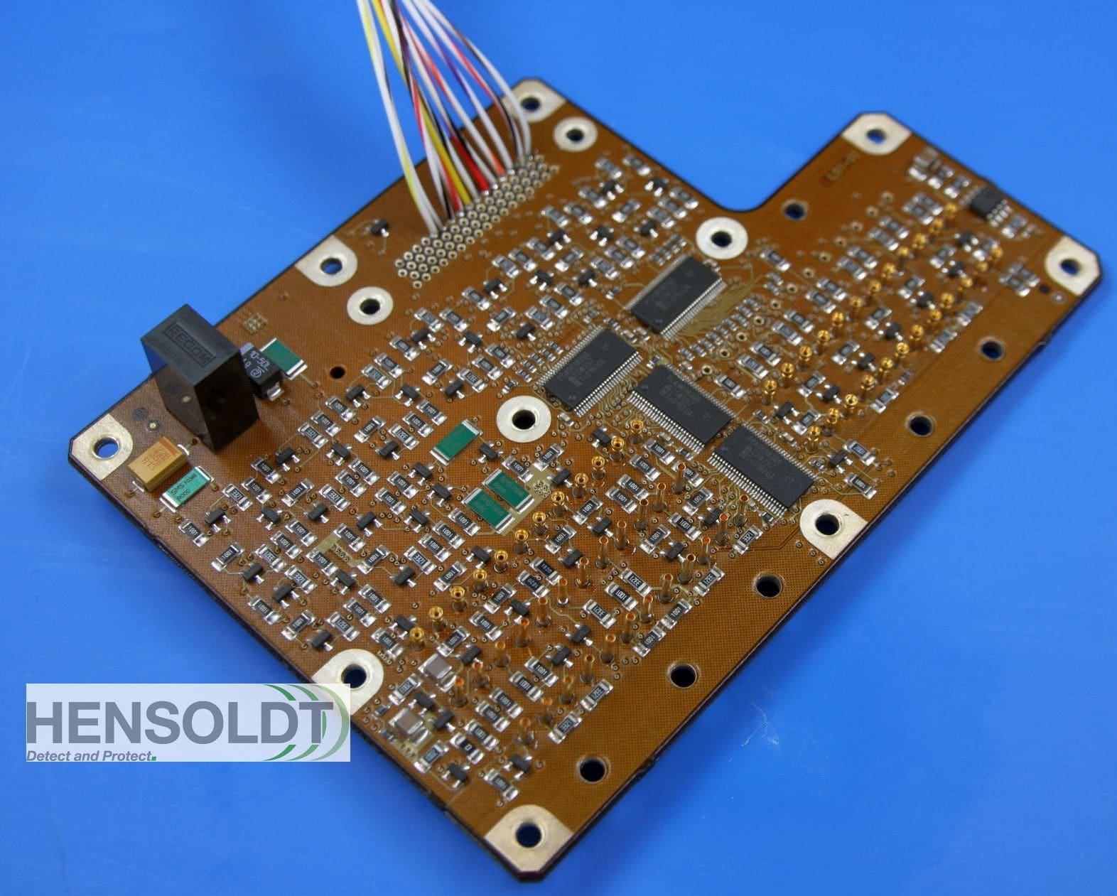
FirstSpear TV

Archive for the ‘Disruptive Tech’ Category

Rare-Earth Element Material Could Produce World’s Smallest Transistors

Thursday, February 13th, 2020

RESEARCH TRIANGLE PARK, N.C. — A material from a rare earth element, tellurium, could produce the world’s smallest transistor, thanks to an Army-funded project.

Computer chips use billions of tiny switches called transistors to process information. The more transistors on a chip, the faster the computer.

A project at Purdue University in collaboration with Michigan Technological University, Washington University in St. Louis, and the University of Texas at Dallas, found that the material, shaped like a one-dimensional DNA helix, encapsulated in a nanotube made of boron nitride, could build a field-effect transistor with a diameter of two nanometers. Transistors on the market are made of bulkier silicon and range between 10 and 20 nanometers in scale.

“This research reveals more about a promising material that could achieve faster computing with very low power consumption using these tiny transistors,” said Joe Qiu, program manager for the Army Research Office, an element of the U.S. Army Combat Capabilities Development Command’s Army Research Laboratory, which funded this work. “That technology would have important applications for the Army.”

The Army-funded research is published in the journal Nature Electronics. The Army is focused on integration, speed and precision to ensure the Army’s capability development process is adaptable and flexible enough to keep pace with the rate of technology change.

“This tellurium material is really unique. It builds a functional transistor with the potential to be the smallest in the world,” said Dr. Peide Ye, Purdue’s Richard J. and Mary Jo Schwartz Professor of Electrical and Computer Engineering.

One way to shrink field-effect transistors, the kind found in most electronic devices, is to build the gates that surround thinner nanowires. These nanowires are protected within nanotubes.

Ye and his team worked to make tellurium as small as a single atomic chain and then build transistors with these atomic chains or ultrathin nanowires.

They started off growing one-dimensional chains of tellurium atoms, and were surprised to find that the atoms in these one-dimensional chains wiggle. These wiggles were made visible through transmission electron microscopy imaging performed at the University of Texas at Dallas and at Purdue.

“Silicon atoms look straight, but these tellurium atoms are like a snake. This is a very original kind of structure,” Ye said.

The wiggles were the atoms strongly bonding to each other in pairs to form DNA-like helical chains, then stacking through weak forces called van der Waals interactions to form a tellurium crystal.

These van der Waals interactions set apart tellurium as a more effective material for single atomic chains or one-dimensional nanowires compared with others because it’s easier to fit into a nanotube, Ye said.

Because the opening of a nanotube cannot be any smaller than the size of an atom, tellurium helices of atoms could achieve smaller nanowires and, therefore, smaller transistors.

The researchers successfully built a transistor with a tellurium nanowire encapsulated in a boron nitride nanotube. A high-quality boron nitride nanotube effectively insulates tellurium, making it possible to build a transistor.

“Next, the researchers will optimize the device to further improve its performance, and demonstrate a highly efficient functional electronic circuit using these tiny transistors, potentially through collaboration with ARL researchers,” Qiu said.

In addition to the Army Research Office, the National Science Foundation, Air Force Office of Scientific Research and the Defense Advanced Research Projects Agency partly funded the work.

By U.S. Army CCDC Army Research Laboratory Public Affairs

SOFWERX Presents The $225,000 Tech Sprint: Hyper Enabled Partner Force

Thursday, February 13th, 2020

In concert with the USSOCOM Joint Acquisition Task Force (JATF), SOFWERX is hosting The $225,000 Tech Sprint: Hyper Enabled Partner Force event, 04-14 May 2020.

Up to 15 selected technologies and their submitters will receive a prize award in the amount of $15,000 to combine and/or integrate their most provocative technologies into the Hyper Enabled Operator (HEO) system. Participants may also have the opportunity to showcase their technology at SOFIC.

The technologies of interest are those that will assist in providing new, novel or provocative solutions in the following categories:

• Linguistical Fluency

• Cultural Fluency

• Social Awareness

• Operational Awareness

• Other Hyper Enabled Capabilities

To get involved, you’ll need to submit NLT 23 March 11:59 PM EST.

For full details, visit www.sofwerx.org/partnerforce

USSOCOM J5 Donovan Group Disruptive Speaker Series – Humans over Hardware: Posturing the SOF Enterprise for the Future

Sunday, January 19th, 2020

Disruptive Speaker Series
Humans over Hardware:
Posturing the SOF Enterprise for the Future

03 March 2020

Are you smarter than a well-oiled machine?

On 03 March, SOFWERX, in collaboration with the USSOCOM J5 Donovan Group, will host a Disruptive Speaker Series entitled “Humans over Hardware: Posturing the SOF Enterprise for the Future,” led by Dr. Lydia Kostopoulos, Strategy and Innovation Advisor for the Donovan Group.

The presentation hopes to stretch the audience’s thinking about how USSOCOM can creatively leverage talent in the context of increased connectivity, demographic changes, new understandings of sovereignty and dynamic threats.

RSVP NLT 24 February 11:59 PM EST

www.sofwerx.org/hoh

See the Latest from Propel, LLC at the Consumer Electronics Show

Monday, January 6th, 2020

Propel, LLC has been doing some spectacular work in eTextiles and they’ve been invited by the Small Business Administration to exhibit at CES.

See them in booth #50000 at this week’s CES in Las Vegas.

SOFWERX – 3D Geospatial Tech Sprint Series

Friday, December 27th, 2019

On 24-28 February, SOFWERX, in concert with USSOCOM Program Executive Office for Special Reconnaissance, Surveillance and Exploitation (PEO-SRSE), will host a 3D Geospatial Tech Sprint to further automate production and dissemination of 3D geospatial data.

Selected software engineers and developers will be afforded the opportunity to collaborate with others to combine their tools for assessment and integration during the week-long event. Selectees will receive an $8,000 stipend for participation in the Tech Sprint.


Submit your technology for review, related to the technology focus areas, to be considered for attendance.

Submit NLT 27 January 11:59 PM EST

For full details, visit www.sofwerx.org/3dgeo

New Algorithm Could Mean More Efficient, Accurate Equipment For Army

Sunday, December 22nd, 2019

RESEARCH TRIANGLE PARK, N.C. (Dec. 19, 2019) –  Researchers working on an Army-funded project have developed an algorithm to simulate how electromagnetic waves interact with materials in devices to create equipment more efficiently and accurately. The algorithm could be used in a wide range of fields – from biology and astronomy to military applications and telecommunications.


Electromagnetic waves exist as radiation of energies from charges and other quantum processes. They include radio waves, microwaves, light and X-rays. Mobile phones communicate by transmitting radio waves.


It takes a tremendous amount of computer simulations to create a device like an MRI scanner that images the brain by detecting electromagnetic waves propagating through tissue. Those simulations can take days or months to identify how the electromagnetic waves will react when they encounter the materials in the device. Because of the cost, there is a limit to the number of simulations typically done for these devices.


With funding from the Army Research Office, in a study, published in the SIAM Journal on Scientific Computing, SMU (Southern Methodist University) researchers revealed a faster algorithm for these simulations. It is a more efficient and less expensive way to predict the behavior of waves.


“We can reduce the simulation time from one month, to maybe one hour,” said lead researcher Wei Cai, SMU Clements Chair of applied mathematics. “We have made a breakthrough in these algorithms.”


“Electromagnetic waves are central to many important applications in sensing, power, and communication. Being able to conduct related simulations faster and less expensively will have many military applications,” said Dr. Joseph Myers, Army Research Office Mathematical Sciences Division chief. ARL is an element of the U.S. Army Combat Capabilities Development Command’s Army Research Laboratory. “For example, this work will help create a virtual laboratory for scientists to simulate and explore quantum dot solar cells, which could produce extremely small, efficient and lightweight solar military equipment.”


The new algorithm modifies a mathematical method called the fast multipole method, or FMM, which was considered one of the top 10 algorithms in the 20th century.


Using this new algorithm, the computer simulations map out how materials in a device like semiconductor materials will interact with light, in turn giving a sense of what a particular wave will do when it comes in contact with that device.


An engineer or mathematician would be able to use this new algorithm to test a device whose job is to pick out a certain electromagnetic wave. For instance, it could be used to test designs for a solar light battery that lasts longer and is smaller than currently exists.


“To design a battery that is small in size, you need to optimize the material so that you can get the maximum conversion rate from the light energy to electricity,” Cai said. “An engineer could find that maximum conversion rate by going through simulations faster with this algorithm.”


The algorithm could also help an engineer design a seismic monitor to predict earthquakes by tracking elastic waves in the earth, Cai noted.


“These are all waves, and our method applies for different kinds of waves,” he said. “There are a wide range of applications with what we have developed.”


The computational system used for this project, the SMU MANEFRAME II, is descended from the Army high-performance computing system “Mana,” formerly located at the Maui HPC Center in Hawaii, and donated and physically moved to SMU through the efforts of ARO and SMU.

By US Army CCDC Army Research Laboratory Public Affairs

US Army Research Institute of Environmental Medicine at Natick Seeks Volunteers for Marksmanship Learning Study

Wednesday, December 11th, 2019

The US Army Research Institute of Environmental Medicine (USARIEM) in Natick, MA is seeking volunteers for a research study investigating the effectiveness of a non-invasive tool that uses mild electrical stimulation of the face to improve learning. The purpose of this study is to determine whether this tool could reduce the amount of time Warfighters need to acquire marksmanship proficiency. If you qualify for participation, you will be asked to answer questions about yourself and your health, complete marksmanship tasks involving a simulated M4 rifle and have your heart rate monitored. Your participation in this study will last approximately 13 hours, which will be spread across 4 days.

To be included in this study, you must be 18 to 30 years of age, exercise at least twice a week, and speak/read English fluently. You cannot have prior military/law enforcement service, and minimal or no prior experience with firearms, including pistols, shotguns, or rifles.

You may receive up to $300 for completing this study if you do not work for the government. Reimbursement may be available for transportation services.

To find out more information please call (508) 206-2432 or email william.h.neumeier.mil@mail.mil

Advanced Manufacturing Techniques Set To Cut Costs, Timelines For US Army

Sunday, December 8th, 2019

ARLINGTON, Va. — The Army’s advanced manufacturing push intends to cut production timelines and costs throughout the lifecycle of systems, said an Army acquisition officer.

“Can you imagine how great it would be if we could just not have any parts in the logistics system, only raw materials, and we would just print the part at the point of need, right?” asked Maj. Gen. David Bassett, program executive officer for Command, Control, and Communications – Tactical, or C3T, during a panel discussion Wednesday.

That vision has become synonymous with advanced manufacturing, he said during the Association of the U.S. Army’s “Hot Topic” forum on Acquisition and Contracting.

Advanced manufacturing forges innovative technologies to “create new, or improved products or processes,” said Paul Mehney, C3T public communications director.

One technique, additive manufacturing, incorporates 3D printing, robotics, artificial intelligence and composite materials. But according to Bassett, that’s just a fraction of what the new push entails.

Over the last several months, C3T project managers have partnered up with the members of the Army’s Command, Control, Computers, Communications, Cyber, Intelligence, Surveillance and Reconnaissance Center — known as the C5ISR — at Aberdeen Proving Ground in Maryland and applied 3D printing techniques for network integration efforts.

At the proving ground, they have been prototyping radio, gateway and server racks, and mounting brackets on lightweight military vehicles to support network enhancement efforts of the Integrated Visual Augmentation System.

“The use of 3D printing enables developers to experiment with form/fit/function of different mounting systems and also allows developers and integrators to quickly incorporate Soldier feedback,” Mehney said.

To enable network connectivity for the Integrated Visual Augmentation System, developers are prototyping an integrated network enhancement kit called the Bloodhound, Mehney said.

Bloodhound is a network communications gateway and data management kit currently integrated onto light vehicles — but it is platform agnostic, he said, meaning it runs equally well on more than one platform.

During recent IVAS Soldier Touchpoint experimentation, infantry Soldiers and Marines provided feedback on the location of network systems on the Bloodhound, and made suggestions to improve form and fit of integrated network components.

“Future IVAS network capabilities may include data synchronization over narrow band SATCOM [Satellite Communications] with up to 75% reduction in component payload size, which will allow for network kit integration into combat and tactical vehicle platforms,” Mehney said.

IVAS network capability integration on the Stryker and Bradley platforms are both already in motion.

“3D manufacturing techniques will allow additional prototypes to be made as more Soldier feedback in development and operations is received, and as additional vehicle platforms are identified for network kit integration,” Mehney said.

Last month, the U.S. Army Combat Capabilities Development Command Soldier Center, in partnership with the University of Maine, procured the world’s largest 3D printer, to further bolster collaboration with industry leaders.

The printer will enable the rapid creation of large products for the Soldier, said Professor Habib Joseph Dagher, Advanced Structures and Composites Center executive director at the college.

Once a design configuration is locked, design plans developed out of advanced manufacturing techniques will be handed to industry for production.

Although the Army fostering of advanced manufacturing methods and materials are in its early stages, the service’s industrial base “must rapidly innovate to keep pace with industry and adversaries exploiting” their own advanced methods and materials, according to an Army statement.

But digital engineering is only the start, Bassett said. “Techniques [with advanced manufacturing] are now available to us that should aid in efficiency, and allow us to build things we never could have envisioned.”

In other words, 3D printing is only a part of advanced manufacturing and it “looks across the entire lifecycle of the system, starting with design, manufacturing and sustainment,” Bassett said.

“If you start to build a system this way,” he said, “when you get to sustainment, you should be able to identify what parts you can manufacture in different ways.”

The Army’s new manufacturing policy is made up of three elements: strategic investment, systematic adoption, and deliberate and thoughtful use, said Brian Raftery, acting deputy assistant secretary of the Army for strategy and acquisition.

Strategic investment must “develop a holistic, threat-based strategy for the investment in and use of advanced methods and materials” and open the door for outside partnership with industry leaders, he added.

The second principle integrates advanced manufacturing technology upfront, and throughout the system’s lifecycle, Raftery said.

And lastly, advanced manufacturing will be deliberate and used thoughtfully, he said. This means it will keep in mind aspects of things like return on investment and intellectual property implications.

Story by Thomas Brading

First photo by SSG Armando R. Limon