SureFire

Archive for the ‘Digitization’ Category

Safran Optics 1 ECOTI

Wednesday, August 5th, 2020

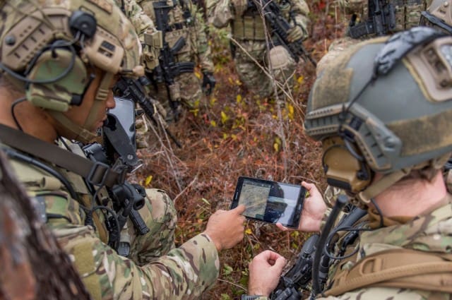
The Enhanced Clip-On Thermal Imager or ECOTI from Safran Optics 1 adds a thermal overlay to the image intensified (I2) NVD scene without modification of existing hardware. It also offers HUD (Heads Up Display) capability that provides real-time, geo-referenced navigation/route execution. When used with Android devices, the NVD becomes a remote display for identifying teammates, targets and route points.

www.optics1.com/products/ecoti-enhanced-clip-on-thermal-imager

Quantum Chip Fabrication Paves Way for Scalable Processors, Producing the Largest Quantum Chip of its Type Using Diamond-Based Qubits and Quantum Photonics

Sunday, August 2nd, 2020

RESEARCH TRIANGLE PARK, N.C. — An Army-funded project marks a turning point in the field of scalable quantum processors, producing the largest quantum chip of its type using diamond-based qubits and quantum photonics.

Millions of quantum processors will be needed to build quantum computers, and new research at MIT and Sandia National Laboratories, funded and managed in part by the U.S. Army Combat Capability Development’s Command’s Army Research Laboratory’s Center for Distributed Quantum Information, demonstrates a viable way to scale-up processor production.

“Building large scale quantum devices will entail both the assembly of large numbers of high-quality qubits and the creation of reliable circuits for transmitting and manipulating quantum information between them,” said Dr. Fredrik Fatemi, Army researcher and CDQI co-manager. “Here, the research team has demonstrated exceptional progress toward reliably manufacturing complex quantum chips with both critical elements.”

Unlike classical computers, which process and store information using bits represented by either 0s and 1s, quantum computers operate using quantum bits, or qubits, which can represent 0, 1, or both at the same time. This strange property allows quantum computers to simultaneously perform multiple calculations, solving problems that would be intractable for classical computers.

The qubits in the new chip are artificial atoms made from defects in the diamond, which can be prodded with visible light and microwaves to emit photons that carry quantum information. The process, which the researchers describe in the peer-reviewed journal Nature, is a hybrid approach, in which carefully selected quantum micro-chiplets containing multiple diamond-based qubits are placed on an aluminum nitride photonic integrated circuit.

“In the past 20 years of quantum engineering, it has been the ultimate vision to manufacture such artificial qubit systems at volumes comparable to integrated electronics,” said Dirk Englund, an associate professor in MIT’s Department of Electrical Engineering and Computer Science. “Although there has been remarkable progress in this very active area of research, fabrication and materials complications have thus far yielded just two to three emitters per photonic system.”

Using their hybrid method, the researchers were able to build a 128-qubit system — the largest integrated artificial atom-photonics chip yet.

The artificial atoms in the chiplets consist of color centers in diamonds, defects in diamond’s carbon lattice where adjacent carbon atoms are missing, with their spaces either filled by a different element or left vacant. In the chiplets, the replacement elements are germanium and silicon. Each center functions as an atom-like emitter whose spin states can form a qubit. The artificial atoms emit colored particles of light, or photons, that carry the quantum information represented by the qubit.

Diamond color centers make good solid-state qubits, but “the bottleneck with this platform is actually building a system and device architecture that can scale to thousands and millions of qubits,” said Noel Wan, MIT research and the paper’s coauthor. “Artificial atoms are in a solid crystal, and unwanted contamination can affect important quantum properties such as coherence times. Furthermore, variations within the crystal can cause the qubits to be different from one another, and that makes it difficult to scale these systems.”

Instead of trying to build a large quantum chip entirely in diamond, the researchers decided to take a modular and hybrid approach.

“We use semiconductor fabrication techniques to make these small chiplets of diamond, from which we select only the highest quality qubit modules,” Wan said. “Then we integrate those chiplets piece-by-piece into another chip that wires the chiplets together into a larger device.”

The integration takes place on a photonic integrated circuit, which is analogous to an electronic integrated circuit but uses photons rather than electrons to carry information. Photonics provides the underlying architecture to route and switch photons between modules in the circuit with low loss. The circuit platform is aluminum nitride, rather than the traditional silicon of some integrated circuits.

Using this hybrid approach of photonic circuits and diamond chiplets, the researchers were able to connect 128 qubits on one platform. The qubits are stable and long-lived, and their emissions can be tuned within the circuit to produce spectrally indistinguishable photons, according to the researchers.

While the platform offers a scalable process to produce artificial atom-photonics chips, the next step will be to test its processing skills.

“This is a proof of concept that solid-state qubit emitters are very scalable quantum technologies,” Wan said. “In order to process quantum information, the next step would be to control these large numbers of qubits and also induce interactions between them.”

The qubits in this type of chip design wouldn’t necessarily have to be these particular diamond color centers. Other chip designers might choose other types of diamond color centers, atomic defects in other semiconductor crystals like silicon carbide, certain semiconductor quantum dots, or rare-earth ions in crystals.

“Because the integration technique is hybrid and modular, we can choose the best material suitable for each component, rather than relying on natural properties of only one material, thus allowing us to combine the best properties of each disparate material into one system,” said Tsung-Ju Lu, MIT researcher and the paper’s co-author.

Finding a way to automate the process and demonstrate further integration with optoelectronic components such as modulators and detectors will be necessary to build even bigger chips necessary for modular quantum computers and multichannel quantum repeaters that transport qubits over long distances, the researchers said.

“The team has made an incredible advance toward the large-scale integration of artificial atoms and photonics and, looking forward, we are very excited for increasingly complex testing of the devices,” said Dr. Sara Gamble, program manager at the Army Research Office, an element of CCDC ARL, and CDQI co-manager. “The modular approach so far successfully demonstrated by the team has enormous promise for the future quantum computers and quantum networks of high interest to the Army.”

By U.S. Army CCDC Army Research Laboratory Public Affairs

*Adapted with permission from an article by Becky Ham, MIT News.

Quantico Tactical Showcases ATAK Enabled Gear from Safran Optics 1

Friday, July 10th, 2020

Aberdeen, North Carolina – July 9, 2020– Quantico Tactical®, the largest North Carolina based federal contractor, is proud to showcase ATAK enabled devices for the dismounted soldier.

Quantico Tactical® has been a longstanding partner with Safran Optics 1. Together these two companies are teaming to offer the latest in Android Tactical Assault Kit, ATAK, enabled devices. ATAK is an app-based technology that identifies and views teammates, targets, and route points. Operators can also see points of interest, such as terrain, topographical elements, and even weather.

The Optics 1 Enhanced Clip-On Thermal Imager, ECOTI, provides unmatched detection capability and situational awareness by adding a long wave infrared thermal overlay on the user’s night vision device, NVD. The ECOTI is a low power consuming thermal sensor that mounts to existing NVD’s.  The ECOTI has a Heads Up Display, HUD, that provides real-time, geo-referenced navigation information.  When combined with an Android device, the NVD becomes a remote display for identifying teammates, targets, and route points.

The Optics 1 Enhanced Clip-On SWIR Imager, ECOSI, is bears the same physical design as the ECOTI, yet provides short-wave infrared, SWIR overlay on to the user’s NVD.  It helps see out-of-band short-wave infrared items like strobes, markers, beacons, and other devices. The ECOSI also integrates augmented reality through the use of ATAK.

“ATAK is a game-changer for properly relaying information,” said Rett Vandenberg, C4ISR Category Manager for Quantico Tactical. “Having the right devices that connect via ATAK can dramatically change the battlefield.”

The Pocket Laser Rangefinder, PLRF25C, is a reconnaissance, surveillance, and targeting device, also by Optics 1 that provides accurate distance and angle measurement. The PLRF25C is a small, lightweight, and ruggedized laser rangefinder that connects via Bluetooth® to wirelessly transmit distance, azimuth, inclination, horizontal distance and vertical distance to a target. The ATAK unit will automatically populate the target location information on the ATAK map.

Bollé Launches First Ever Augmented Reality Sunglass Experience For Smartphones

Tuesday, June 23rd, 2020

New AR Technology Allows Users to Experience Bollé Phantom lenses on their Smartphone and Purchase From a Participating Retailer.

Lyon, France, (JUNE 23, 2020) – Bollé, maker of the most innovative lenses in the world is forever changing the way people try and buy sunglasses. With the introduction of an exclusive Augmented Reality Sunglass experience, shoppers can now try-out Bollé’s flagship Phantom lens technology without ever having to physically touch the glasses. 

Partnering with QReal and M7 Innovations, Bollé’s AR experience is a first for the sunglass industry. Within Instagram, the demonstration invites users to try out Bollé’s Phantom lens through one of the brand’s iconic models – the Chronoshield. After seeing the glasses on their face, users simply flip their camera from selfie-view to front-facing and Phantom lenses are superimposed on their actual view. Users then introduce sunglass effects like high contrast, anti-fog, and light-adaptive into their real surroundings to see Phantom lenses in action. Once users select a lens that suits their style and needs, they can search for a retailer that carries Bollé. 

“AR is routinely used for try-on and certainly enhances the buying experience. But AR for try-out, this is a first,” said Louis Cisti, Vice President of Global Marketing for Bollé Brands. “In the new normal of retail, Bollé recognizes that safety is now the most important thing. Consumers demand shopping encounters that minimize physical interaction. However, when it comes to buying premium sunglasses, they still have high expectations and expect to see tangible benefits. Bollé’s AR try-out does all that heavy lifting. Shoppers get to see perceivable performance benefits before making a purchase.” Cisti continued.

Using AR, users will experience several unique Bollé lens features that demonstrate Phantom’s superiority for spring skiing, cycling, running and more: 

• Light Adaptive Technology: the user is presented with a slider that allows them to change their exposure, making the scene brighter or darker. They watch Phantom’s molecular photochromic filter adapt to changes in ambient light. 

• Platinum Anti-Fog Treatment: The user’s view begins to fog up, simulating the fogging that occurs from sweat while riding, hiking, or spring skiing. Fog condenses outside the glasses, but the view through the sunglasses remains crystal clear, mimicking the real-world performance Phantom Lenses in a perspiring situation.

• High Contrast: The scene outside the glasses remains natural, but the user is able to experience improved color and depth perception as they look through the Phantom lenses. 

For the Try On part of the experience users will be able to see how they look in the Bollé Chronoshield, a new take on an original style from the 1980s. The Chronoshield offers an extra wide field of view, ideal for visual comfort and protection against wind or debris. Venting ensures the lenses never fog up and the adjustable Thermogrip nose-pads and temple tips gives a custom fit while making sure they stay in place.

To try-out Phantom Lenses using this augmented reality experience, users can either click on a QR code that will be included in Bollé marketing materials or may visit this link using their: Merged Single Lens Experience

Integrated Visual Augmentation System Update

Friday, June 19th, 2020

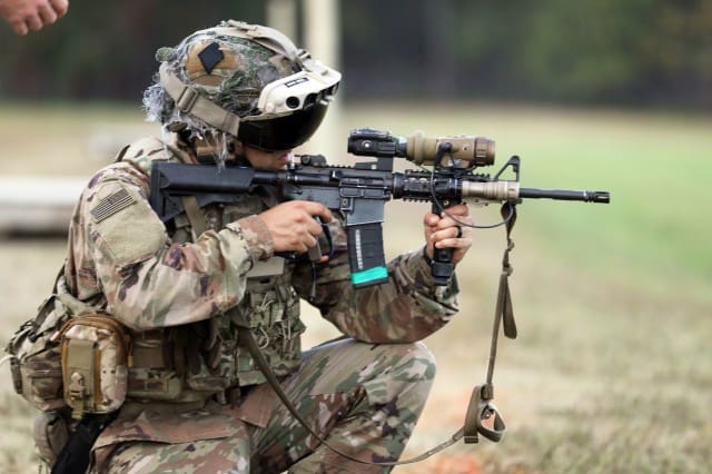
Here one of the latest photos of the US Army’s Integrated Visual Augmentation System, a which fuses image intensification and thermal imaging with Augmented Reality overlays. It’s built by Microsoft.

Interestingly, the form factor is pretty similar to the Soldier Integrated Protective Ensemble headborne subsystem from the early 90s.

Here’s an update from the Program Office.

Team IVAS Continues to Deliver Despite COVID Obstacles
“I can absolutely say that today we are on track to meet a fourth quarter ‘21 delivery for our first unit equipped.”
– COL. Chris Schneider, PM IVAS

FORT BELVOIR, Va.– Cutting-edge modernization efforts come with their own set of challenges, and COVID-19 has ensured that there are no exceptions.

Program Executive Office (PEO) Soldier’s Project Manager Integrated Visual Augmentation System (PM IVAS) continues to leverage the team’s unique structure, talents, and culture to contribute to the force’s readiness, even with the additional challenges presented by COVID-19.

Mark Stephens, PM IVAS Director of Acquisition and Operations, and Jared Walega, PM IVAS Test Director, highlighted how problem solving, routine distributed work solutions, modular architecture design, Soldier Centered Design (SCD), and Supply Chain Risk Management (SCRM) have allowed the project flexibility during the COVID pandemic.

Stephens emphasized how Team IVAS has applied efficient problem-solving skills from the project’s inception.

“Senior defense officials recognized the erosion in close combat capabilities and saw an immediate need to ensure overmatch for our dismounted force,” said Stephens. “Congress recognized the requirement and reprogrammed funds to start IVAS in FY19. Within six months from the Secretary of Defense’s approval in late May, Team IVAS awarded multiple Other Transaction Agreements to industry and kicked off IVAS before Christmas 2018.”

Team IVAS has rapidly solved problems ever since. This includes the successful integration of partners from around the country. Because the team overcame this initial obstacle, remote work is now routine.

The distributed team has built and relied on a digital infrastructure to manage the mission from any physical location. Therefore, they are able to maintain the mission even with the obstacles COVID has presented.

“When COVID hit we had already established a solid Integrated Product Team [IPT] Battle Rhythm using long distance collaboration methods like SharePoint, TEAMs, and Power BI,” Stephens said. “Using TEAMs over the past 18 months allowed video teleconferencing, sharing document collaboration, and reviewing our program management dashboards, so all our leaders were battle tested”.

Secure remote tools have allowed for continued IVAS prototyping through Army Enabled Tests (AET) even while team members are quarantined at home.

“We also implemented a practice of what we call Army Enabled Testing that allows us to get updates from our partners, test the updates in a safe environment, and provide feedback. This methodology helps us manage our performance risks, and not have to wait until Soldier Touchpoint 3 [STP 3] to discover problems,” said Stephens.

Team IVAS’ dynamic problem solving and reliable remote infrastructure guaranteed that aspects of testing continued to ensure minimal overall impacts to the program’s timeline.

“As COVID-19 impacted the organization, the Test Directorate determined we could still conduct a thorough AET with focus on Rapid Target Acquisition (RTA), Tactical Assault Kit (TAK), Synthetic Training Environment (STE), and other necessary capabilities while maintaining requisite social distance and implementing COVID-approved decontamination procedures for the Heads Up Displays (HUD),” said Walega.

“We have a dispersed team that is capable of downloading the latest software build and loading it onto their HUDs. This process has enabled remote testing of software builds and the ability to provide rapid feedback to Microsoft to include live fire video, data, and assessments,” Walega added.

The continued AET testing and iteration of specific IVAS capabilities through the COVID pandemic has been largely based on the Soldier feedback collected at every stage in development over the last 18 months.

“Soldier Centered Design (SCD) was developed in IVAS as a combination of Human Centered Design and tailored acquisition best practices,” said Walega. “SCD focuses on current Soldier and Marine input throughout the entire development process to prevent engineers and developers from building a product that does not meet the priorities of our warfighters.”

The process puts emphasis on making a product that Soldiers will enjoy using to increase their lethality in training and on the battlefield.

According to Walega, “If a Soldier loves and uses IVAS, then we have provided a system that has much greater capability than the current kit.”

In order to ensure that IVAS will truly maximize Soldier lethality, intentional Soldier feedback at every design and decision point has been a program priority.

“We have collected over 23,000 hours of Soldier feedback,” said COL. Christopher Schneider, Program Manager IVAS. “Because we’ve got so much feedback, we’re highly confident in the current design and STP 3.”

The Soldier-centric approach has turned out to be a key asset to the program during the change in normal operations. Though large scale events such as the IVAS STP 3 will shift due to COVID restrictions, the team has reorganized the internal program schedule so that IVAS is not delayed in deploying to the warfighter.

The team is reordering the intensive hardware and software design reviews that were initially planned for after STP 3, and is leveraging their ingenuity, remote tool infrastructure, and plethora of Soldier feedback to expedite the hardware design review to before the October event. This will allow the formal software design sprint to be completed after STP 3, and both designs to be finalized during Capability Set 4 iterations.

“We wouldn’t have the flexibility that we do, frankly, if we hadn’t been doing Soldier Touchpoints, user juries, user studies, and human factors engineering excursions throughout the last 18 months of the program,” said Schneider.

Though the pandemic has impacted every aspect of the program, including supply chain logistics, industry partners have continued to support with solutions.

“With the advent of the Coronavirus, the supply chain risk management strategy has taken on a new level of importance,” said Nicholas Pate, PM IVAS Manufacturing Engineer.

“IVAS vendors have worked tirelessly to assess, analyze, and make quick decisions to avert imminent delays. Luckily, the PM IVAS supply chain strategy, from the very start of the program, has always been to mitigate risk by avoiding sole sources of supply, cultivating multiple sensor vendors, and ensuring parallel paths of supply,” said Pate.

To date, IVAS vendors have been able to react quickly to minimize negative impacts from the Coronavirus.

“Microsoft, as well as the low light and thermal sensor vendors, delivered preliminary supply chain information on critical components for early risk mitigation assessment on the IVAS supply chain,” Pate added. “This information ensures that quality and security controls are implemented to ensure a stable and sustainable supply chain.”

As Team IVAS continues to overcome COVID’s obstacles, leadership is unwavering in its dedication to the safety of both Soldiers and the team.

“We really took a deliberate thought process and approach to moving the Soldier Touchpoint into October,” said Schneider. “We wanted to make sure that we had the opportunity to get it right.”

Overall, every decision has been made with the safety of the team and readiness of Soldiers as top priorities. Though STP 3 is now taking place in October at Fort Pickett, Va., the rest of the program deliverables remain on track.

“I can absolutely say that today we are on track to meet a fourth quarter ‘21 delivery for our first unit equipped,” said Schneider.

Story by Courtney Bacon.

SOFWERX – Trusted Capital AI Virtual Venture Day Starting 24 June 2020

Wednesday, June 17th, 2020

The Office of the Secretary of Defense (OSD) Trusted Capital, in concert with the United States Special Operations Command (USSOCOM), the Joint Artificial Intelligence Center (JAIC), and the Department of Energy (DOE), will host an AI-focused Trusted Capital Virtual Venture Day.

Trusted Capital events are designed to bring together DoD-critical companies and capital providers to align their existing capabilities with national security interests.

The goal is to facilitate funding of companies with critical technology to provide risk mitigation against adversarial influence in supply chains and funding channels.

Trusted Capital maximizes the public-private partnership model. The U.S. government screens capital providers and companies for national security risks prior to offering participation in Venture Days and the Trusted Capital program. Eligible companies are firms offering technologies and capabilities critical to national security and seeking to secure sources of funding in support of the defense industrial base. Eligible capital providers are investment groups that support U.S. national security sectors that align with their investment portfolio.

Approximately 10 qualifying AI companies will deliver their pitches and funding needs to trusted providers of capital weekly over the course of several weeks. If your organization is accepted in Trusted Capital, you will receive an opportunity to prepare a five-minute pitch video with one minute at the end for questions from the capital providers and acquisition community.

This program will be administered on a first-come, first-serve basis for those companies that qualify to participate in the Trusted Capital Marketplace (TCM).

AI sectors of interest:
• Autonomous Vehicles
• Machine Vision and Image Recognition
• Machine Learning
• Robotics and Scale Automation
• Navigation System
• Language Processing and Recognition

Potential participants will undergo the due diligence required to pass a national security review for entrance into the Trusted Capital Venture Day and Trusted Capital Marketplace.

Submission Deadline: 22 June 11:59 PM EST

Visit events.sofwerx.org/trustedcapital to enter.

New 5G Switch Provides 50 Times More Energy Efficiency Than Currently Exists

Saturday, May 30th, 2020

RESEARCH TRIANGLE PARK, N.C. — As 5G hits the market, new U.S. Army-funded research has developed a radio-frequency switch that is more than 50 times more energy efficient than what is used today.

With funding from the Army Research Office, an element of the U.S. Army Combat Capabilities Development Command’s Army Research Laboratory, researchers at The University of Texas at Austin and the University of Lille in France, have built a new component that will more efficiently allow access to the highest 5G frequencies, in a way that increases devices’ battery life and speeds up how quickly users can do things like stream HD media.

Smartphones are loaded with switches that perform a number of duties. One major task is jumping back and forth between different networks and spectrum frequencies: 4G, WiFi, LTE, Bluetooth, etc. The current radio-frequency switches that perform this task are always running, consuming precious processing power and battery life.

“Radio-frequency switches are pervasive in military communication, connectivity and radar systems,” said Dr. Pani Varanasi, division chief, materials science program at ARO. “These new switches could provide large performance advantage compared to existing components and can enable longer battery life for mobile communication, and advanced reconfigurable systems.”

The journal Nature Electronics published the research team’s findings.

“It has become clear that the existing switches consume significant amounts of power, and that power consumed is useless power,” said Dr. Deji Akinwande, a professor in the Cockrell School of Engineering’s Department of Electrical and Computer Engineering who led the research. “The switch we have developed can transmit an HDTV stream at a 100GHz frequency, and that is an achievement in broadband switch technology.”

The new switches stay off, saving battery life for other processes, unless they are actively helping a device jump between networks. They have also shown the ability to transmit data well above the baseline for 5G-level speeds.

Prior researchers have found success on the low end of the 5G spectrum – where speeds are slower but data can travel longer distances. This is the first switch that can function across the spectrum from the low-end gigahertz frequencies to high-end terahertz frequencies that could someday be key to the development of 6G.

The team’s switches use the nanomaterial hexagonal boron nitride, a rapidly emerging nanomaterial from the same family as graphene. The structure of the switch involves a single layer of boron and nitrogen atoms in a honeycomb pattern sandwiched between a pair of gold electrodes. Hexagonal boron nitride is the thinnest known insulator with a thickness of 0.33 nanometers.

The impact of these switches extends beyond smartphones. Satellite systems, smart radios, reconfigurable communications, and Internet of Things, are all examples of potential uses for the switches. In addition, these switches can be realized on flexible substrates making them suitable for Soldier wearable radios and communication systems that can benefit from the improved energy efficiency for longer battery life with faster data speeds as well as other defense technologies.

“This will be very useful for radio and radar technology,” Akinwande said.

This research spun out of a previous project that created the thinnest memory device, also using hBN. Akinwande said sponsors encouraged the researchers to find other uses for the material, and that led them to pivot to RF switches.

In addition to the U.S. Army, support through a Presidential Early Career Award for Scientists and Engineers, the U.S. Office of Naval Research and The National Science Foundation’s Engineering Research Center funded the research. The Texas Nanofabrication Facility partly fabricated the switch and Grolltex, Inc., provided hBN samples.

By U.S. Army CCDC Army Research Laboratory Public Affairs

Samsung Introduces Next Generation of Tactical Mobility with the Galaxy S20 Tactical Edition

Thursday, May 21st, 2020

Mission-ready smartphone solution provides operators with the power to achieve their objectives in any tactical environment.
 

RIDGEFIELD PARK, N.J. – MAY 20, 2020 – Samsung Electronics America, Inc. today introduced the Samsung Galaxy S20 Tactical Edition (TE), a mission-ready smartphone solution tailored to the unique needs of operators in the federal government and Department of Defense (DoD).  With a highly customized software and feature set, the Galaxy S20 TE can operate seamlessly with a range of existing peripherals and supports the requirements of tactical and classified applications, especially those designed to help operators navigate complex terrain, expansive distances, and the potential loss of communication with command units. Galaxy S20 TE also introduces DualDAR architecture, which delivers two layers of data encryption based on the NSA standards to secure up to top-secret level data for classified missions.

“The development of this solution is a result of coordination and feedback received from our Department of Defense customers and partners,” stated Taher Behbehani, Head of the Mobile B2B Division, SVP and General Manager, Samsung Electronics America. “The Galaxy S20 Tactical Edition provides the warfighter with the technology that will give them an edge in the field, while providing their IT teams with an easy-to-deploy, highly secure solution that meets the demands of their regulated environment.”

Galaxy S20 TE offers federal program managers and executive officers an easy to manage and deploy mobile solution that works with a broad range of technologies and is backed by the assurance of the defense-grade Samsung Knox mobility platform. It harnesses the most sought after tools of Samsung’s premium Galaxy devices in a unique, easy-to-use configuration.

Helps Operators Stay Connected in Multi-domain Operations. Galaxy S20 TE easily connects to tactical radios and mission systems, out of the box, ensuring seamless operations. Multi-ethernet capabilities provide dedicated connections to mission systems, while network support for Private SIM, 5G, Wi-Fi 6 and CBRS ensure a connection is maintained throughout multi-domain environments.

Provides complete, accurate real-time situational awareness. Galaxy S20 TE caters to the unique needs of military operators, through customization of numerous device features. A night-vision mode allows the operator to turn display on or off when wearing night vision eyewear, while stealth mode allows them to disable LTE and mute all RF broadcasting for complete off-grid communications. Operators can easily unlock the device screen in landscape mode while it’s mounted to their chest, and quick launch their most commonly used apps at the push of a button.

One Device for All Mission Requirements. When in the field, operators need a lightweight, easy to carry device that doesn’t weigh them down, yet offers the power they need to complete the mission. With its powerful 64-bit Octa-Core processor, Galaxy S20 can support the running of multiple mission applications in the field (ATAK, APASS, KILSWITCH, BATDOK) so operators can access the intelligence they need. Galaxy S20 TE also includes powerful Samsung DeX software, which offers a PC-like experience when connected to a monitor, keyboard, and mouse. With DeX, operators can use the device for completing reports, training or mission planning when in vehicle or back at the base.

Certified and secure for Special Operations. Galaxy S20 TE is built on Samsung Knox, the defense-grade mobile security platform that protects the device from hardware through software layers.  DualDAR architecture further secures the device with two layers of encryption, even when the device is in a powered off or unauthenticated state. This multi-layer, embedded defense system helps Galaxy S20 TE meet the most stringent regulated industry requirements, including NSA’s Commercial Solutions for Classified (CSFC) Component’s List, and Mobile Device Fundamental Protection Profile (MDF PP) as laid out by the National Information Assurance Partnership (NIAP). Galaxy S20 TE comes out of the box approved for use within the Department of Defense (DoD) using the Android 10 Security Technical Implementation Guide (STIG) as laid out by the Defense Information Systems Agency (DISA).

The Samsung Galaxy S20 TE will be available in Q3 2020 through select IT channel partners.  For more information on Galaxy S20 TE, please visit www.samsung.com/TacticalEdition. For more information about Samsung Government, please visit www.samsung.com/us/business/by-industry/government.